Main Arm Board
Authors
Board Design: Brendan Parvin with review and assistance by Shin Umeda
Documentation: Brendan Parvin
Active Revisions
Revision 1, 8/21/2024: Implementation Specifics
Revision 2, 9/18/2024: Implementation Specifics
-Removed can hotfix as it is not needed
-Fixed micromod connector
-Changed positioning of U4 and JTAG connector to not interfere with optional C4
-Length matched JTAG traces
Revision 3, 10/19/2024
-Fixed USB_DET connection
Summary
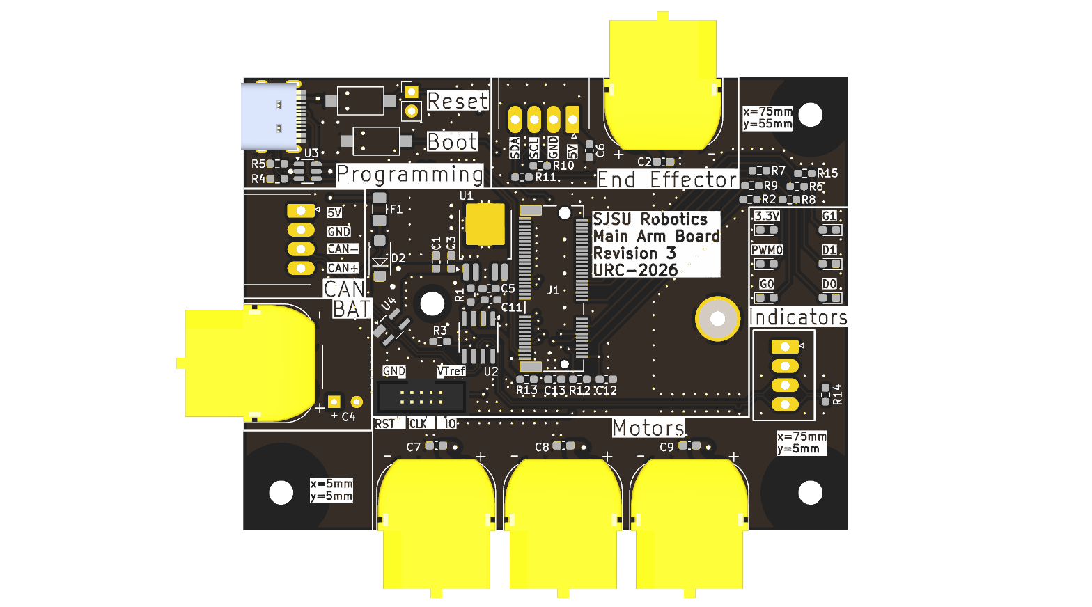
This board is both a power distribution and controller board for the arm. It is the interface between the chassis CAN bus and all arm modules.
Application Description
There are five main application notes:
1. It accepts 40V power, CAN, and 5V from the chassis with connectors on the left side of the board
2. It outputs 40V power and CAN to the arm motors with connectors on the bottom of the board
3. It outputs 40V power, 5V, and I2C up the arm using connectors on the top of the board
4. It contains a micromod connector to control the arm — and allows programming using either USB-C or JTAG
Implementation Details
Mounting Points
There are three main M3 mounting holes located at the corners of the board. These are shown in the image below.
There is one additional M3 mounting hole located near the left middle of the board. This hole was included just in case, but is not in a very standard location.
Arm Outputs
There are two connectors that output up the arm towards the end effector. One of these is a 40V passthrough intended to power any high-power motor devices. The other connector carries both 5V and I2C. As such, all communication from the end effector to the main arm board should be done through I2C. Note that the 40V, 5V, and I2C lines are not galvanically isolated. In order to avoid large ground loops, the 5V connector's ground should be connected to the 40V connector's ground anywhere that both are used.
Indicator LEDs
The board contains 5× user programmable indicator LEDs + 1× 3.3V power-on indicator LED. LEDs are labeled with their respective Micromod Connector pin. However, it might be necessary to consult the datasheet of your respective micromod processor board to determine the actual pin connection. Each LED draws approximately 1-2mA while on.
Micromod Programming
All Micromod boards support programming through the on board USB-C port. Note that the USB-C port will power the 5V rail, outputs, and inputs on the board. Ensure that there are no loads greater than 500mA connected to 5V.
In addition, a 10-pin JTAG Connector is included. This connector is wired only on ARM-based Micromod processor boards. 5V power must be supplied through another connector to program over JTAG.
40V Bypass Capacitors
All 40V Bypass capacitors are left as DNP in this design because it is likely that any 40V device will already contain sufficient input capacitance. However, if large voltage transients are measured, a through-hole electrolytic capacitor can be added adjacent to the 40V input connector (low-frequency filtering), and additional 0603 capacitors can be added adjacent to every output connector (high-frequency filtering).
Schematic Diagrams
Programming
Connectors
Micromod and Supporting Circuitry
Old Revision Implementation Specifics
Revision 1
Can Hotfix
On the back of the board are two solder jumpers that provide a hotfix in case CAN TX and CAN RX are swapped on the specific Micromod processor board.
Note that the micromod pin should not be soldered to both TX and RX at the same time. The default connection is Pin 43 <-> TX, Pin 41 <-> RX and is shown below.
Power Error
- Pin 74 of the micromod is supposed to be connected to 3.3V, but is instead connected to the ground.
To solve this problem, you must remove the pin from the micromod connector before soldering it to the board.
USB Error
- Pin 9 should be connected to VBUS, but was left unconnected
To solve this problem, you must solder a wire or resistor to an exposed power joint as shown.
Revision 2
- Pin 9 should be connected to VBUS, but was left unconnected
To solve this problem, you must solder a wire or resistor to an exposed power joint as shown.